Custom Probe Stations
There are several methods that have been used for detection of electron flow problems in semiconductor devices such as leakage,
gating problems and localized heat build up due to Ohmic shorts. These have been addressed by Emission Microscopy,
Fluorescence Microthermography, Raman Spectroscopy and Liquid Crystal with polarization.
1. LIQUID CRYSTAL COATING
With polarized light will allow the failure analysis engineer to see a localized heat buildup on a device of greater than 10 degrees C.
For this reason it is really only used for gross thermal failures.
2. RAMAN SPECTROSCOPY
There will be a Stokes peak with Raman scanning as a much smaller 0.2 degrees C temperature differences are encountered.
This method is not practical for a production related failure analysis since it is a slow time consuming method.
3. FLUORESCENCE MICROTHERMOGRAPHY
This method is done with a coating of Europium-tritheno-polymerthacolate which is commercially available. It requires a high sensitivity
camera and fluoresces in the visible red region. It is lower cost than Emissiom microscopy and will cover most of similar defects.
It claims to have 0.1 degree C sensitivity, but like the above methods it depends on heat signatures.
4. EMISSION MICROSCROPY
This method is the more expensive one, but is the fastest and cleanest. As it does not require any coating to be applied to the wafer.
It will show leakage and gating problems in the Lower part of the NIR spectrum (below 1000nm) and thermal signatures at 1800 nm.
For this type of usage a camera such as Mercadtelluride has been used, with the Mitutoyo NIR ULWD objectives, which transmit out to 1800nm.
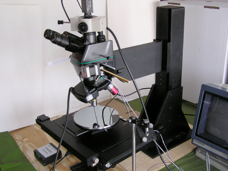
CHIP STACKING TRANSFER STATION
For the process of stacking structures of unlike materials in precise placement and alignment on a semiconductor chip,
we offer our Chip Stacking or Van Der Waals Transfer Station.This setup has 2 independent XYZ stages: one is to move the platen on
which the micropositioners sit and the other is to move the heated chuck, independent of the platens.
The XY stage that moves the heated chuck also has a precision fine rotational stage.
One micropositioner has a custom spring loaded clamp to hold a microscope slide which holds the chip, in contact with the hot chuck,
while other materials or structures will be transferred or stacked on the chip. Since this is done manually (in a research situation)
a probe station type microscope on a rigid stand, with long working distance optics facilitates this operation.
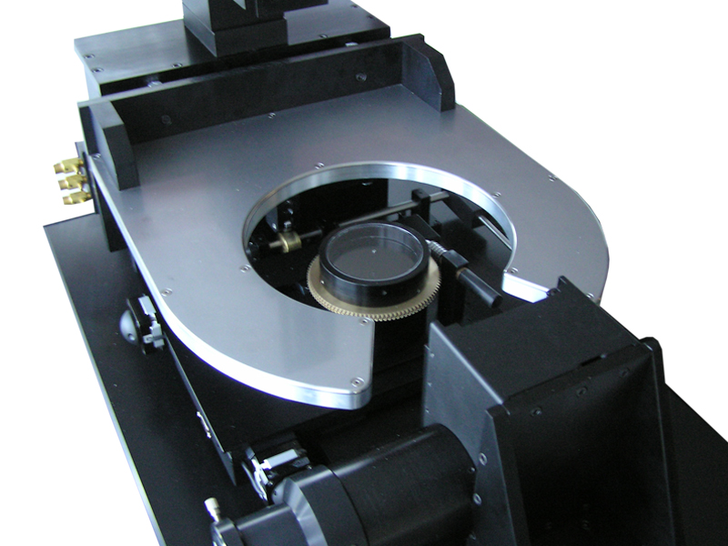
SOLAR, SENSOR AND BACKSIDE LED APPLICATIONS
Some applications require backside illumination or spectral sensing of
a wafer while probing the top of the wafer. This requires a transparent chuck.
We use a 2 piece fused silica vacuum chuck, so that illumination
or sensing can be done from 250nm to 1800nm.
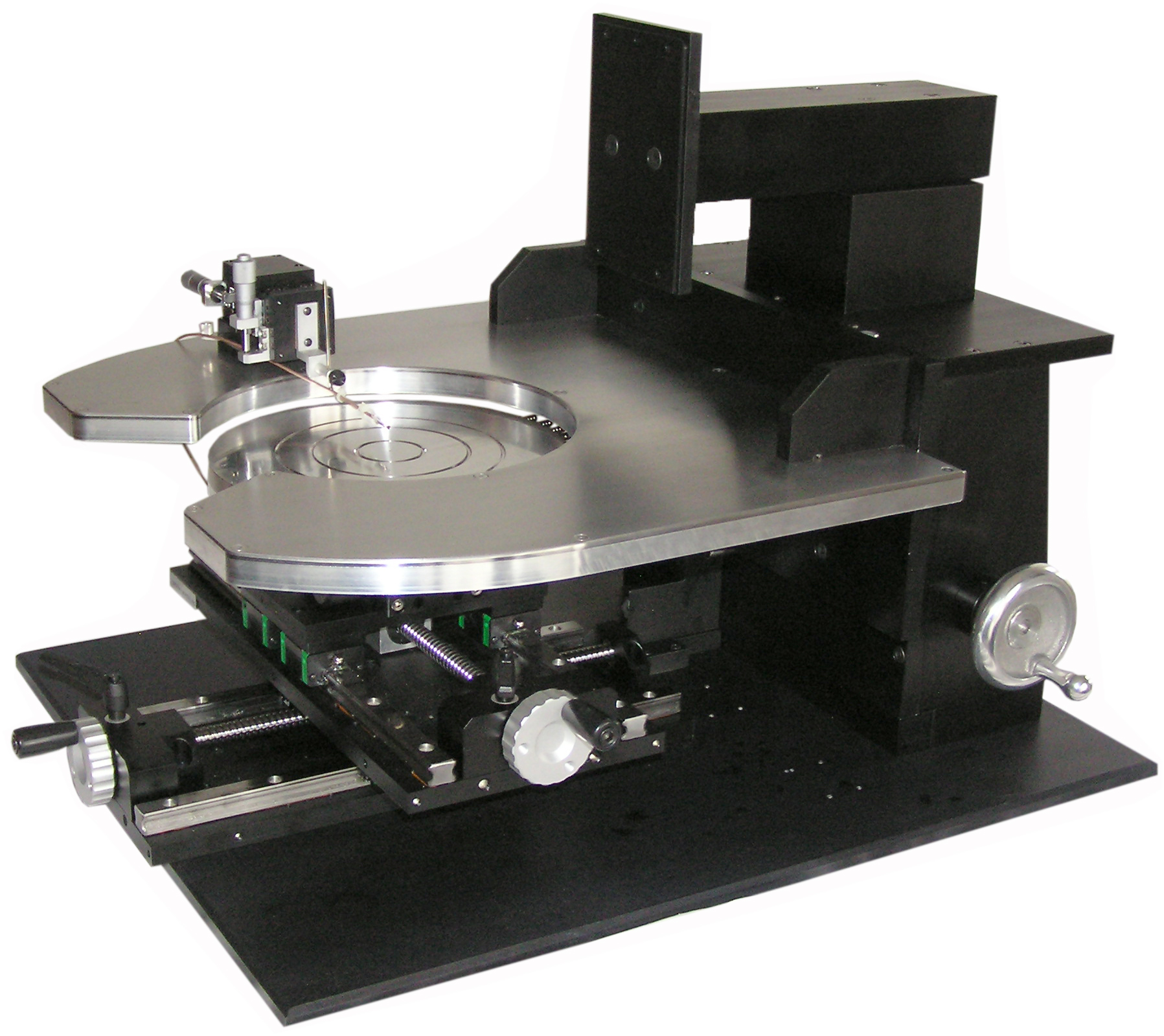
BU8-17-FPF WIDE PLATEN
PROBE STATION
Our standard 8″ chuck probe station comes with a 14″ wide platen and a lever
action up/down quick lift platen mechanism. Our customer had an application
that required a 17″ wide platen with a precision fine feed lift. We created the precision fine feed lift using a ball screw mechanism with a worn gear drive. Only
a few ounces of torque is required to lift the heavy platen with very fine resolution.
For the 8″ vacuum chuck with a 360 degree fine theta, we used a Ball Screw driven
precision cross roller bearing 8″ x 8″ stage. The platen has a magnetic stainless
steel top which is ideal for our BU-075 on/off magnetic base micropositioners.