High Voltage Applications
In High Voltage Applications the main problem is arcing which will occur at 1 kilovolt (KV) and above.
There have been two approaches to avoid this:
1. Immerse the device under test (D.U.T) in fluorinert.
2. Do the test (probing) under High Vacuum.
As a result, we developed our High Vacuum Probe Station for device testing at 10 KV.

HIGH VACUUM PROBER
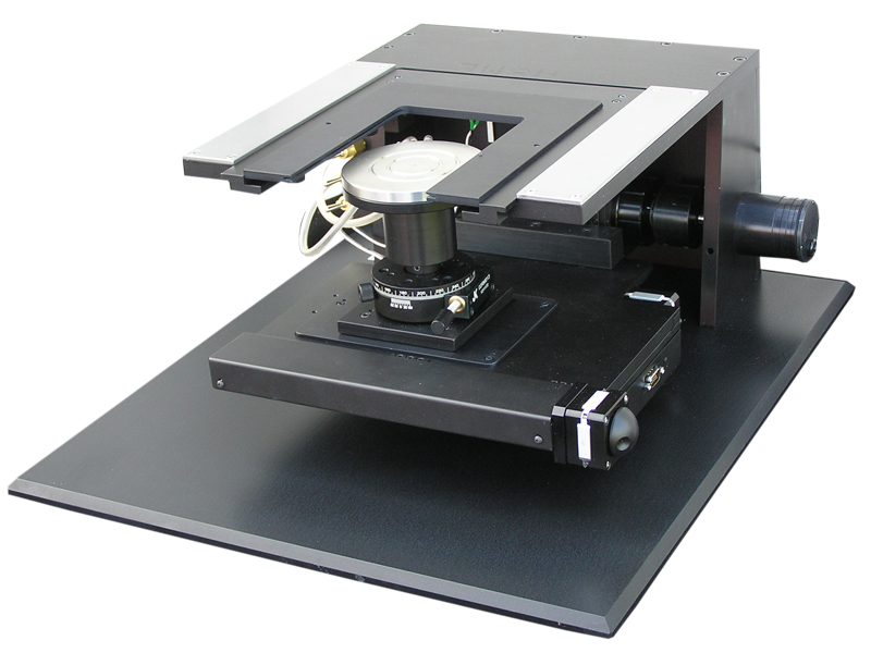
For aerospace and a variety of applications it may be necessary to test devices or wafers under moderate to high vacuum conditions. The system in this picture was designed for a 10 KV application. The high vacuum prevents arcing. In this case we used ceramic probe holders and a Peltier Cooled Stage and a thermal InSb camera to see heat signatures in a SiC device under high voltage. These high vacuum systems were PC automated. In this picture, the chuck is a Peltier Cooled Stage, used to enhance heat signatures for the device under test. An NIR sensitive camera was used for imaging. On other systems we used heating chucks.
These are available from 200-600 degrees C.
These are available from 200-600 degrees C.
HIGH VACUUM PROBER
High Vacuum chamber closed, showing 3mm thick sapphire window for viewing in the NIR above 2000nm. In another case we installed a 3mm fused silica window for viewing below 1,800nm. This system used a thermal heating chuck.

HIGH VACUUM PROBER
This is a compact low profile automated probe station, designed to drop into the high vacuum chamber shown. In this case to be used for laser trimming under vacuum.
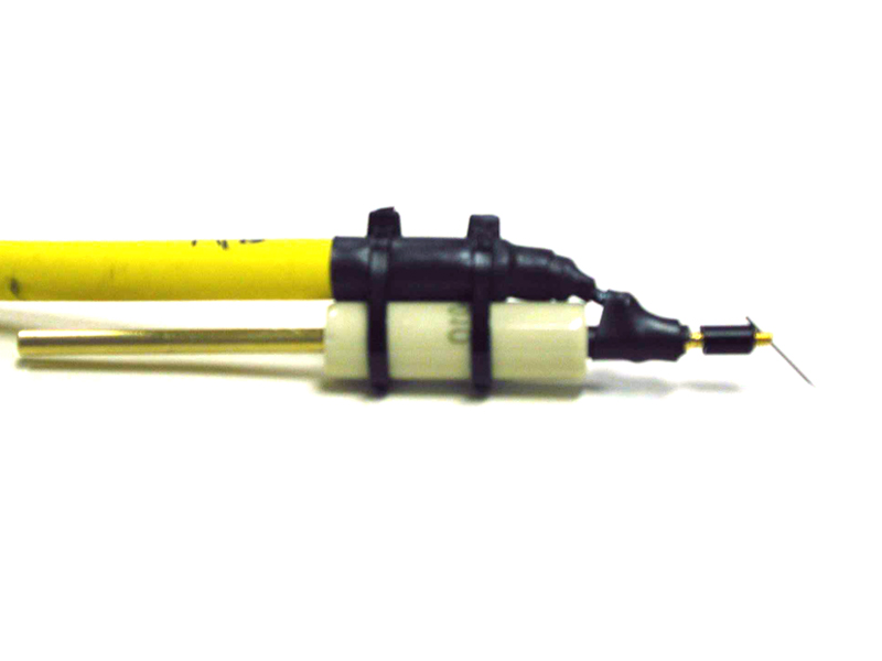
HV PROBE HOLDER
To avoid the arcing that will occur at and above 1KV we
recommend using our high vacuum prober to be found on the
High Vacuum Prober Page.
recommend using our high vacuum prober to be found on the
High Vacuum Prober Page.