Field Emission Microscope / Fluorescence Microthermography
There are several methods that have been used for detection of electron flow problems in semiconductor devices such as leakage,
gating problems and localized heat build up due to Ohmic shorts. These have been addressed by Emission Microscopy,
Fluorescence Microthermography, Raman Spectroscopy and Liquid Crystal with polarization.
1. LIQUID CRYSTAL COATING
With polarized light will allow the failure analysis engineer to see a localized heat buildup on a device of greater than 10 degrees C.
For this reason it is really only used for gross thermal failures.
2. RAMAN SPECTROSCOPY
There will be a Stokes peak with Raman scanning as a much smaller 0.2 degrees C temperature differences are encountered.
This method is not practical for a production related failure analysis since it is a slow time consuming method.
3. FLUORESCENCE MICROTHERMOGRAPHY
This method is done with a coating of Europium-tritheno-polymerthacolate which is commercially available. It requires a high sensitivity
camera and fluoresces in the visible red region. It is lower cost than Emissiom microscopy and will cover most of similar defects.
It claims to have 0.1 degree C sensitivity, but like the above methods it depends on heat signatures.
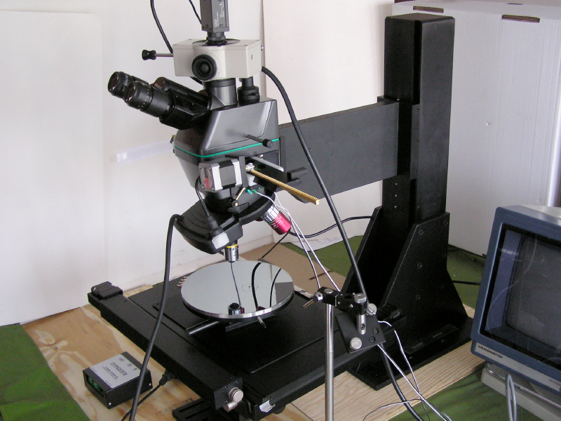
4. EMISSION MICROSCROPY
This method is the more expensive one, but is the fastest and cleanest. As it does not require any coating to be applied to the wafer.
It will show leakage and gating problems in the Lower part of the NIR spectrum (below 1000nm) and thermal signatures at 1800 nm.
For this type of usage a camera such as Mercadtelluride has been used, with the Mitutoyo NIR ULWD objectives, which transmit out to 1800nm.
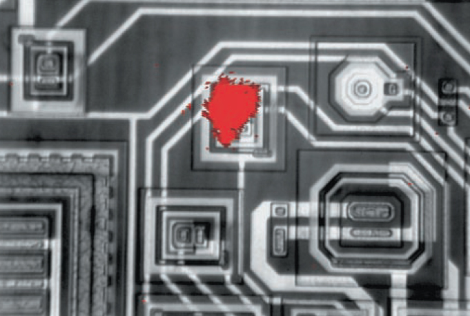
EXAMPLE OF PHOTON EMISSION
Resulting from high electron activity due to defect.
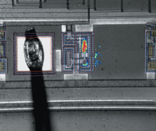
EXAMPLE OF ELECTRON LEAKAGE
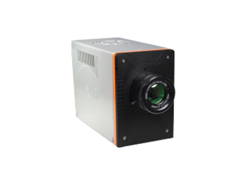
XEVA-FPA CAMERA
High sensitivity NIR camera.
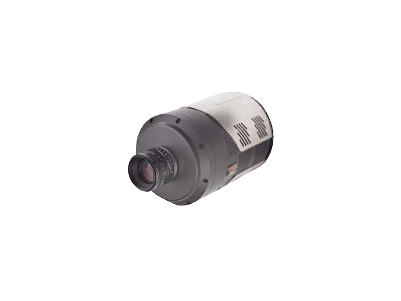
PIXIS 1024 CAMERA
High sensitivity NIR camera.
LIGHT TIGHT ENCLOSURE
For light sensitive and very low current applications.